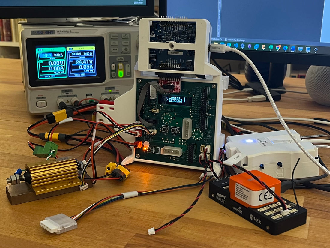
To develop our 6S battery management system, we have developed a hardware testing station, which is able to program the BMS and test all the critical functionality. This is all controlled by a single Python program, that tells the ST-Link to upload certain bin files during certain points of the initiation process. It communicates with the voltage supplies and a 16-channel multimeter through LXI. A resistive load serves in testing the MOSFETs. To calibrate the BMS measurements, the Python program communicates with the BMS through its external i2c connection. The 3D-printed frame consists of two main parts: one that holds the testing PCB permanently and the other pushes the BMS and its test points onto the pogo pins. A simple clamping device secures the BMS in place during the process.

If you want to design a hardware testing station yourself, here comes a detailed introduction:
The design of your hardware testing station begins with the design of the hardware you want to test (device under test = DUT). Look at every signal that might be of interest and add a test point. You will always want all communication channels and all voltage supplies. Also, add test points for every signal that leaves the board so you can simulate signals entering and leaving the board. If you need to program one or more of the I2C on board, make sure that you have all the necessary pins connected. If you have free GPIOs on your MCU, you might just add a test point to them, this can be a great help in the debugging process. You will also want to power the board through test points, so make sure that there are enough test points to carry the current. This is specified in the datasheet of the pogo pins that you are using, but 200mA to 500mA should be roughly what is possible. If you have buttons on your board, you can add extra test points for them and then simply add an external button on the pogo-pin board to simulate the functionality. Don’t forget your reference signal which will often be ground. Factor in that you will not have the tightest tolerances, so choose your test points as big as reasonable. In most cases, bigger than 2mm will not be necessary. Make sure that the test points are well-spaced. Check in advance how much spacing the pogo-pins will need. If your test points are placed too tight you might not be able to assemble the pogo pins later. All test points need to be on the same side.
Keep in mind that the pogo pins are spring-loaded, placing a bulk of them on one side of the board and only a few on the other side will result in a very uneven force. It is a good strategy to have the pogo-pins spaced out, so the forces on the board are roughly equal. When placing components on the other side opposite your test points, keep in mind that you still need to push the board down. Therefore, you need areas on which you can push. Keep areas of a minimum of 5x5mm free of component placement. Routing in those areas does not harm. You will need at least three of those areas if you can place them strategically, but the more the better. Those areas should also be close to where your test points are placed. This minimizes the mechanical stresses that are introduced to the board.
Begin developing your testing station only after you have completed your hardware design.
Start by building your schematic. Add all the test points you have on your DUT as pogo pins, and headers for each to easily measure the signals. Depending on your DUT you will need to add protection circuitry to prevent the DUT itself but also the testing equipment in case of a malfunction. If your device has high capacitance, there might be enough energy stored to cause damage. Protection circuitry encompasses overvoltage, over-current, and reverse polarity. Know what you want to test. At least one power supply and a multimeter should be necessary. If you need to program an MCU or other ICs on your DUT, check which cables you have to do that. Most programmers come either with a JTAG connector or have female header pins for each signal. You can adjust the design to what you already have. Each signal that you might want to measure needs a header pin. Add adequate connectors for power coming to your board. The same if you have power leaving the board. External NTCs can be simulated by means of standard resistors. If you want to simulate different temperatures, you can add jumpers to different resistor values. Add buttons for buttons that you want to simulate and add buttons for resetting circuitry of MCUs that might not be present in the product.
Start your layout by placing the pogo pins in the exact same coordinate as the test points of your DUT, you can open a second instance of your ECAD software to have both designs open at the same time. When placing components for your testing hardware, keep in mind that you will want to add labels that can be easily read. When placing connectors and header pins, keep in mind that cables will be connected to them, and you will still want to reach eventual buttons on the board. Make sure to add cutouts if you have LEDs or displays on your DUT that you will want to see. When routing signals, you will need to obey the same rules as with any PCB design. However, your testing PCB is likely not as dense and therefore not very complicated to route. Mind your references, as you do not want to introduce errors to your measurements that originate on your testing hardware. Add adequate mounting holes and space around the mounting holes for the contact area and screws.
When ordering the testing PCB, mind that the force of the pogo-pins might deform it. You can counteract the deformation by ordering a higher-thickness PCB.

When you have ordered your testing hardware it is time to design the mechanics. The mechanics should be designed to be easily 3D-printed and general design rules for designing for 3D-printing should be applied. Choose a compression clamp to push your DUT to the pogo pins. Depending on the size of your DUT you might need several clamps. Export both your testing PCB as well as your DUT to a CAD software of your choice. A simplified design of your compression clamp will also help.
Arrange the PCBs together in your CAD software and align them based on the pogo-pin placement. The distance of the PCBs should be so that the pogo pins are compressed but not all the way through. 2/3 of the compression distance should be okay but have a look in the datasheet to know more. The first part you are going to design holds the test hardware. Use tight tolerances. The tolerance of your DUT can be a bit higher and there should be chamfers or filets to facilitate putting the DUT in. The second part you design will be between your DUT and the compression clamp. By giving this mart more thickness, it will bend less and apply the forces more equally on the DUT. Ensure that the second part only touches fee PCB areas on your DUT and no components. Add extensions to the second part, so it interlocks with the first part and is centered to its position when clamped. You can also add chamfers and fillets to facilitate the closing process. Now add the compression clamp to the design and add mounting holes to the first part you designed. You can add extra features, to sort cables by means of cable ties or feat to have the assembly stand in a certain direction when under test and when swapping the DUT.
You will need tight tolerances for your assembly to work. You might have to print several parts and adjust the tolerances each time until you find the perfect fit for the testing hardware as well as the DUT.
Designing software for your testing station needs to be very specific to your DUT and the lab equipment that you have available. Most lab equipment will be able to communicate through LXI. Create a Python class for each device you are communicating with. This way your code will be better readable and easier to change. Make a sketch of the testing algorithm that you need. This can be on paper or with drawing software like DrawIO. Before starting the whole testing algorithm test the individual functions and ensure they are working as intended.
If you need assistance with designing such testing hardware, feel free to contact us. We offer engineering services and can help you with your project.